January
9, 2006
Nanomaterials
bloom
Much of today's nanotechnology is the result of materials science
research, and materials science, in turn, is a cross-disciplinary combination
of chemistry, physics and engineering. The ability to control the composition
of materials at the nanoscale makes it possible to produce materials that
have very specific electrical, optical, magnetic and chemical properties.
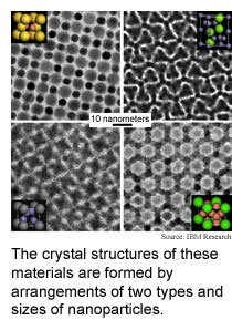 Researchers from IBM Research, Columbia University and the University
of Michigan have found
that a technique for engineering materials at the nanoscale, dubbed binary
nanoparticle superlattices, has a considerably greater range of possibilities
than previously thought. They produced dozens of materials by arranging
two types of nanoparticles that differ by composition and size into various
crystal structures.
Researchers from IBM Research, Columbia University and the University
of Michigan have found
that a technique for engineering materials at the nanoscale, dubbed binary
nanoparticle superlattices, has a considerably greater range of possibilities
than previously thought. They produced dozens of materials by arranging
two types of nanoparticles that differ by composition and size into various
crystal structures.
Previous simulations that treated nanoparticles as simple spheres
showed limited potential for the technique, but the the laws of physics
for particles of various substances in the 1 to 10 nanometer range proved
otherwise. The researchers produced 11 different crystal structures, for
instance, by changing the arrangement of 6.2 nanometer lead selenium nanoparticles
with 3 nanometer palladium nanoparticles.
The materials could eventually be used to make inexpensive computer
chips, photonic crystals, data storage devices and chemical catalysts.
(Structural Diversity in Binary Nanoparticle Superlattices, Nature,
January 5, 2006)
Nano gives solar 2-for-1
There are two ways to make solar cells more practical: decrease
their prices and increase their efficiency. The lion's share of solar
cell advances have been in the former camp -- making solar cells less
expensive by making them from inexpensive materials like like plastics
and zinc oxide. A couple of recent developments, however, show that there's
a lot of potential for boosting the amount of electricity the average
solar cell produces.
Solar cell's work by converting sunlight's photons into electrons
that can be put to practical use as electricity.
Los Alamos National Laboratory researchers have shown
that it is possible to produce two or more electrons from a single photon
using many kinds of semiconductor materials, not just the more exotic
lead selenium of initial carrier multiplication experiments. (See Solar
crystals get 2-for-1, TRN, May 19/26, 2004)
The researchers' tests show that many kinds of semiconductor nanocrystals
can be used to coax more than one electron from a photon, and that the
size of the minuscule particles rather than their composition is key to
the phenomenon.
Solar cells made with semiconductor nanocrystals could use carrier
multiplication to boost solar efficiency to 60 percent, according to the
researchers. Today's state-of-the-art solar cells are less than 40 percent
efficient.
(Effect of Electronic Structure on Carrier Multiplication Efficiency:
Comparative Study of PbSe and CdSe Nanocrystals, Applied Physics Letters,
December 19, 2005)
Email shows it's who you know
Social networks are notoriously difficult to study. Fortunately,
computer networks are changing that.
Columbia University researchers studied
more than 14 million email messages generated by more than 43,000 members
of a large university over the course of a year. The study tracked pairs
of email correspondents based on attributes like gender, age, departmental
affiliation, status, and years in the community, and classes taught or
attended.
The study looked at the factors that influence whether strangers
form a connection via mutual acquaintances. As it turns out, key factors
are the strength of ties to mutual acquaintances, number of mutual acquaintances,
and having shared classes, while individual attributes don't have a significant
influence in forming connections.
Shared friends and shared activities win out over shared characteristics,
at least in universities.
(Empirical Analysis of an Evolving Social Network, Science,
January 6, 2006)
Sensor sees spark of life
Increasingly, and in many ways, computer chip technology is proving
invaluable to the life sciences.
Researchers from the University of Manchester in England and the
Institute for Microelectronics Technology in Russia have made an electric
field sensor that detects the electric charge of a single electron,
and does so at room temperature rather than less practical cryogenic temperatures.
The sensor is a semiconductor device that can measure electric
fields in spaces as small as 100 nanometers, which is about one tenth
the size of an E. coli bacterium.
The researchers used the sensor to measure the electrical responses
of individual yeast cells to changes in their environment. The sensor
could be used in biochips and laboratory equipment that monitors biological
activity.
(Submicron Sensors of Local Electric Field with Single-Electron
Resolution at Room Temperature, Applied Physics Letters, January
2, 2006)
Bits and pieces
A microfluidic device measures subtle changes
in pressure like when a cell membrane ruptures, an infrared camera
system aligns
images of organs projected onto human bodies, a test
with a spacecraft nearly 15 million miles from Earth shows the potential
for interplanetary laser-based communications.
RSS Feeds: News Blog Books New: TRN's Internet Services TRN's Jobs Center News: Research News Roundup Research Watch blog Features: View from the High Ground Q&A How It Works Buy an ad link |
|
| Advertisements: |
|
Ad links: Clear History
Buy an ad link
|
TRN
Newswire and Headline Feeds for Web sites
|