 |
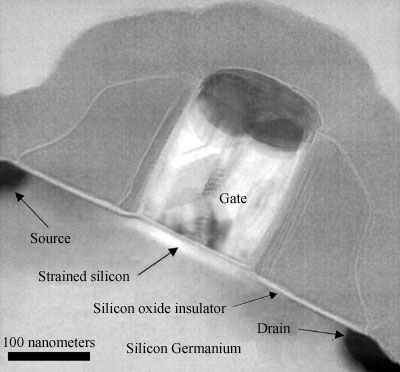
| Description: This prototype transistor uses a layer of strained silicon to speed the flow of electrons from its source electrical contact to its drain contact. The gate produces an electric field that switches on the flow of electrons between the source and drain. |
| Source: IBM Research |
| Story: Stressed
silicon goes faster TRN June 13/20, 2001 |
| TRN Categories: Semiconductors |
| Form: Still |
|
TRN
Newswire and Headline Feeds for Web sites
|
© Copyright Technology Research News, LLC 2000-2008. All rights reserved.