Stressed
silicon goes faster
By
Kimberly Patch,
Technology Research NewsMuch of the work toward making computer chips faster is aimed at shrinking the size of the transistors that make up their circuits in order to reduce the distance current has to flow. This work has steadily doubled computer speeds every 18 months during the past couple of decades in the phenomenon known as Moore's Law.
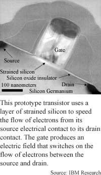
IBM researchers have found another way to speed signals that could increase chip speeds up to 30 percent. The technology could show up in products as soon as 2003, according to the researchers. Instead of shrinking transistors, the researchers altered the structure of silicon in a way that allows electrons to pass through it with less resistance.
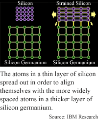
The method strains, or stretches portions of the silicon crystal, reshuffling atoms so that they are spaced further apart. The researchers did this by depositing a very thin layer of silicon on top of a thicker slice of silicon germanium, which has atoms spaced further apart than silicon. Because atoms from different crystals tend to align when they're in contact with one another, the silicon atoms stretch to match the germanium atoms.
One consequence of the strain is a change in the silicon atoms' valence bands, which are the paths that conduct electrons around the atoms' nuclei. Instead of the usual six valence bands that conduct similarly, the strained silicon has four higher energy bands and two lower energy bands, said Jeff Wesler, manager of high-performance semiconductor technologies at IBM Research.
The key to the speed increase is electrons, like water flowing downhill, seek out lower energy bands. And because those bands offer less resistance it takes less voltage to push them through. "It causes the electrons to be able to move with a higher velocity," said Wesler.
The lower resistance is due to a couple of strange quantum effects: the electrons effectively weigh 30 percent less when going through those bands; they also meet with less vibrational energy from the nucleus of the atom, which causes them to scatter less and thus flow more quickly than in the higher energy bands.
If an electron traveling through silicon were instead a pool ball traversing a pool table, the researchers' method would speed the ball by making it lighter so that the same amount of energy transferred through the pool cue would send it further. The method would also partially clear the ball's path so it would get to the other side sooner simply because it bumped into fewer balls on its way.
Although the researchers' method doesn't change the actual speed of individual electrons, it increases electrical current because using less energy to move an electron translates to more electrons moving through using the same amount of energy; at the same time the straighter path reduces the average distance an electron travels. Although electrons in circuits move somewhere between 5 and 10 million centimeters per second, their effective speed is considerably less. "Much of the electrons' speed is in lots of different directions because they don't tend to move in a straight line," said Wesler.
The changes cause the current of electrons to flow up to 70 percent faster in the large experimental chips the researchers are using; this should translate to a 35 percent faster current and a 25 to 30 percent speed increase in commercial-size chips, according to Welser. "Using it on transistors that are scaled-down to the type of dimensions we use today there are a lot of other competing effects, so the net result is something on the order of 30 to 35 percent. Assuming that we are continuing to do our job in scaling our wires and other things correctly, we should be able to translate a lot of this directly into chip performance -- 25 to 30 percent," he said.
The same effect can be used to produce chips that run at the same speed as today's, but use about 25 percent less power, which could prove useful in the growing portable electronics market, said Wesler. "You can trade that off either way, you can either... use a lower voltage and get lower power... or use the same voltage and push them through faster," he said.
The method has been under development for several years. The technology should show up in high-end servers near the end of 2003, and will be spread across other, high-volume product lines about a year later, said Wesler.
Long term, the method could be used for quantum dot memories. Sandwiching the strained silicon with its lower energy bands between layers of silicon germanium could produce quantum wells that trap electrons for this purpose, said Wesler.
It's a novel idea that could prove useful, said Carolyn Matzke, a microdevice technologies research engineer at Sandia National Laboratories. "Film strain has been a problematic issue and I'm happy to see that someone is exploring a useful application," she said. The method is tricky, however, she said. "The device reliability, especially gate oxide integrity, should be very carefully addressed up front," she said. The method's eventual usefulness depends on how its reliability stacks up with existing technologies, and how difficult it proves to manufacture, she added.
The researchers are currently working to find ways to consistently produce a layer of silicon germanium that is free of defects, or irregularities in the way atoms are positioned, Wesler said. "When you grow these really thick layers of silicon germanium... you get a whole bunch of defects that want to form. So the challenge is figuring out ways to control these [because] the silicon will just follow whatever defects are already there in the template."
A defect free layer of silicon germanium is difficult to produce because the material has to be relatively thick -- about one micron -- in order to strain a very thin .02-micron layer of silicon. Today's chips use silicon wafers that are about one tenth of a micron thick, and they are easier to keep defect free simply because they contain less material. Defects cause problems in electronics because they make materials behave unpredictably.
Once the challenge of manufacturing thick layers of silicon germanium is worked out, the chips will fit well with existing chip manufacturing processes, said Wesler. "The making of the initial material is obviously more difficult. But the nice thing about it is once you have the substrate... you can run that through a normal manufacturing line, so we can use the same tools and essentially the same manufacturing process," he said.
The IBM researchers developing the strained silicon process are Lijuan Huang, Jack Chu, Sherif Goma, Christopher D'Emic, Steven. Koester, Donald Canaperi, Patricia Mooney, Steven Cordes, James Speidell, Rhonda Anderson, Ken Rim, Steven Koester, Michael Hargrove, Jack Chu, Patricia M. Mooney, John Ott, Thomas Kanarsky, Paul Ronsheim, Meikei Ieong, Alfred Grill, and H.-S. Philip Wong.
They are scheduled to present a pair of papers on the research at the Symposium on VLSI Technology today in Kyoto, Japan. The research was funded by IBM.
Timeline: < 3 years
Funding: Corporate
TRN Categories: Semiconductors
Story Type: News
Related Elements: Technical paper, "Strained Si NMOSFETs for High Performance CMOS Technology," and "Carrier Mobility Enhancement in Strained SI-on-Insulator Fabricated by Wafer Bonding," Symposium on VLSI Technology in Kyoto, Japan, June 13, 2001.
Advertisements:
June 13/20, 2001
Page One
Stressed silicon goes faster
Artificial synapses copy brain dynamics
DNA device detects light signals
Lightwaves channel atoms to make chips
Process promises better LCD production
News:
Research News Roundup
Research Watch blog
Features:
View from the High Ground Q&A
How It Works
RSS Feeds:
News
Ad links:
Buy an ad link
| Advertisements:
|
 |
Ad links: Clear History
Buy an ad link
|
TRN
Newswire and Headline Feeds for Web sites
|
© Copyright Technology Research News, LLC 2000-2006. All rights reserved.