DNA conducts
By Ted Smalley Bowen, Technology Research NewsWhile popular and scientific attention has gravitated to efforts at mapping DNA and feats of DNA-scale micro-engineering, the comparatively simple act of coating a mica slab with the most famous of complex molecules could prove an effective way of creating a network that has useful electrical properties.
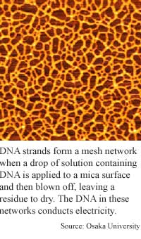
Using a method that might strike grade-school art students as familiar, researchers at Osaka University have found that putting a drop of highly concentrated DNA on mica and blowing it off can leave a residue that amounts to a networked layer of DNA molecules.
The method is a step toward creating high-density electronic devices, and ultimately integrated circuits made of DNA, said Tomoji Kawai, a professor of physics at Osaka University.
In exploring these networks of DNA the researchers found that guanine-cytosine-based DNA shows p-type, or positive electrical properties, according to Kawai. DNA molecules can contain any mix of two types of base pairs: thymine-adenine and guanine-cytosine.
An n-type object uses negatively charged electrons to carry current. A p-type object carries current using positively charged holes, or gaps where an electron could fit. Connections between the two types allow current to flow in a single direction, giving rise to components like transistors and diodes. "[This] means that these networks can be used as p-n junctions and p-n diode[s]," Kawai said
With these electrical traits, DNA could be used to build transistors, which are the basic building blocks of integrated circuits. "The junctions of DNA can be used as three terminal devices," Kawai said.
The way DNA conducts electricity is complex, according to Kawai. It depends on the different reduction-oxidation potentials of the bases, and the distance between bases. A molecule in reduction attracts electrons and in oxidation it sheds electrons. The DNA base guanine is the most easily oxidized of the bases, meaning it can become positively charged, or gain holes. Once this happens, the charge can be passed along a chain of bases, according to Kawai.
The group made their conduction observations by attaching five-nanometer gold particles to specific complementary base pairs within the DNA networks. These gold particles served as one electrode, while the probe tip of an atomic force microscope provided the second contact.
The question of whether DNA conducts electricity is controversial. According to Cees Dekker, a professor of applied physics at the Delft University of Technology in the Netherlands, the results are puzzling. "After two to three years of research on the intrinsic resistance of DNA I've become rather pessimistic that one can use bare DNA as molecular wires," he said.
Others, however, are cautiously optimistic. "The results fit my intuition of the base composition affect on resistivity," said Danny Porath, a physicist at the Center for Nanoscience and Nanotechnology at Tel Aviv University. He added, however, that more experiments are needed to confirm the results.
The researchers have also changed the thickness of the DNA network using electrical current or irradiation, Kawai said.
To create the networks, the researchers applied a solution of synthetic linear DNA in de-ionized water to freshly-cut muscovite green mica and blew it off after about a minute. "The droplet is blown out from the surface," said Kawai.
The result is a network of DNA molecules that is mainly a single layer, and at the edges of the network the DNA molecules are linked together, according to Kawai.
The researchers controlled the size of of a network by changing the concentration of the DNA solution and the time it remained on the substrate, according to Kawai. The resolution, or mesh size, of a network depends on the length of its DNA, he said. The researchers have made networks as large as 2 centimeters square with 10- to 100-nanometer mesh.
The droplet method should scale reliably, said Kawai. "It is easy to make larger area networks. Just increase the substrate area."
The network structure could be used in combination with a bio-chip, such as a DNA chip or a protein chip, within a few years, said Kawai. A DNA memory device could be made within five to ten years, Kawai said.
Kawai's research colleagues were Takahashi Kanno, Hiroyuki Tanaka, Norio Miyoshi. They described their work in the April 2000 Japan Journal of Applied Physics, the research was funded by the Japanese Ministry of Education, Sports and Culture.
Kimberly Patch contributed to the reporting of this story.
Timeline: 5-10 years
Funding: Government
TRN Categories: Semiconductors and Materials; Biological, Chemical, DNA and Molecular Computing
Story Type: News
Related Elements: Technical paper "A New Self-Fabrication of Large-Scale Deoxyribonucleic Acid Network on Mica Surfaces," Japan Journal of Applied Physics, April, 2000
Advertisements:
February 7, 2001
Page One
DNA conducts
DNA induced to superconductivity
Muscles tapped for virtual input
Tiny treads move minuscule robot
Proposal would marry atom and photon
News:
Research News Roundup
Research Watch blog
Features:
View from the High Ground Q&A
How It Works
RSS Feeds:
News
Ad links:
Buy an ad link
| Advertisements:
|
 |
Ad links: Clear History
Buy an ad link
|
TRN
Newswire and Headline Feeds for Web sites
|
© Copyright Technology Research News, LLC 2000-2006. All rights reserved.