HP
maps molecular memory
By
Eric Smalley,
Technology Research NewsBuilding electronic components like computer memory out of individual molecules would yield extraordinarily powerful and cheap computers. But figuring out how to mass-produce the devices is a tremendous challenge.
Assuming the devices can be built, another monumental challenge remains: how do you talk to them? The wires in today's semiconductor devices are about 100 times too large to fit molecular devices.
Researchers at Hewlett-Packard Company have found a random chemical process that bridges the gap.
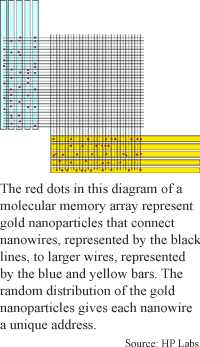
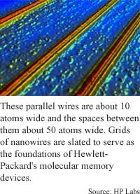
The researchers' proposed molecular memory unit is a grid of tiny wires, each about two nanometers in diameter. A nanometer, which is one millionth of a millimeter, is about 10 carbon atoms long. A single molecule at each junction of the nanowires is an electrically activated switch whose on and off states represent the ones and zeros of computing. On one side the tiny wires extend past the grid.
To connect the memory unit to the outside world, the researchers plan to randomly sprinkle nanometer-size gold particles on the sections of the nanowires that extend past the grid and then lay down a set of larger wires on the gold particles at right angles to the nanowires. This second set of wires, each about 200 nanometers in diameter, is large enough to make a connection to the macroscopic world.
By using the right concentration of gold particles, the researchers can ensure that half of the junctions between the larger wires and nanowires hold individual particles. "There's a purely random, 50-50 chance that a nanowire is connected to a big wire by a dot," said Philip Kuekes, a computer architect and senior scientist at HP Labs.
Some of the junctions the larger wires make with a single nanowire will have connections and others won't. For instance, a nanowire connected randomly to 10 larger wires might have connections at the first, second, fourth, seventh and ninth, but not the third, fifth, sixth, eighth and tenth larger wires. If a connection represents a one and no connection a zero, this particular string of junctions would represent the binary number 1101001010. "So there's a random binary number. That's a unique address for the nanowire," said Kuekes.
In order to read or write to a memory array of nanowire junctions, you have to be able to identify each junction, which holds one bit of data. The binary numbers of the two nanowires that intersect at a junction combine to make a unique address for the junction.
If it were possible to assign addresses directly to the nanowires, 10 larger wires would be sufficient to name 1,000 nanowires because 210 is 1,024. But because the addresses are assigned randomly, many of them are duplicated. Increasing the size of the addresses by adding more larger wires reduces the number of duplicated addresses, said Kuekes.
The trick is finding the balance between getting as few duplicated addresses as possible and keeping the number of larger wires manageable. The HP researchers found that four times the log of the number of nanowires is optimal, said Kuekes. The log of a number is how many times you have to multiply 10 to get the number. For example, the log of 1,000 is three because 103 equals 1,000. By this formula, 12 larger wires can address 1,000 nanowires, 16 can address 50,000 nanowires, 23 can address 500,000 nanowires, 24 can address a million nanowires and 36 can address a billion nanowires.
To find all the unique nanowire addresses, the HP researchers came up with a computer algorithm that measures electrical resistance as the larger wires are switched on and off. Because each nanowire crosses a unique sequence of larger wires, it has a unique electrical signature. The process essentially builds a map of the nanowire grid, said Kuekes.
Figuring out how to exchange information between molecular scale devices and conventional electronic devices is perhaps the most fundamental molecular electronics problem, said Tom Jackson, a professor of electrical engineering at Pennsylvania State University. "The HP [proposal] points in that direction," he said. "It's significant [but] there are limitations to it."
One problem is that simply connecting the nanowires to the larger wires with gold nanoparticles would yield fixed connections that could not be turned on and off, making it impossible to electrically identify each nanowire, Jackson said. To get around this problem, the HP proposal calls for adding a molecular switch similar to those in the memory unit to each of the nanowire-larger wire junctions linked by a gold nanoparticle.
Putting a molecular switch on each nanoparticle and then forming connections between the nanowires and larger wires without crushing the molecular switches is a major but not insurmountable challenge, Jackson said.
Researchers at Hewlett-Packard and the University of California at Los Angeles are beginning a four-year project to build a 16 kilobit memory device using the molecular memory technology, said Kuekes.
The researchers' ultimate goal is to pack 100 gigabits, or 100 billion bits, into one square centimeter of chip space using the molecular memory technology, he said. That's at least 1,000 times more than is possible using standard semiconductor technology, he said.
The molecular memory addressing system could be used in practical devices in five to ten years, according to Kuekes. Beginning in five years the technology could be used in niche products that require very low-power, very high-density memory, he said. The molecular memory technology should match the data capacity of standard semiconductor memory in nine or 10 years, he added.
Kuekes' research colleague was Stan Williams of Hewlett-Packard. They received a United States patent for their research on July 3, 2001. The research was funded by the Defense Advanced Research Projects Agency (DARPA) and Hewlett-Packard. Their ongoing work is also funded by DARPA and HP.
Timeline: 5-10 years
Funding: Government, Corporate
TRN Categories: Biological, Chemical, DNA and Molecular Computing; Integrated Circuits
Story Type: News
Related Elements: United States patent, "Demultiplexer for a molecular wire crossbar network," number 6,256,767, July 3, 2001
Advertisements:
July 18, 2001
Page One
HP maps molecular memory
Cartoons loosen up computer interfaces
Virtual view helps run tiny factory
Bioengineers aim to harness bacterial motion
Lasers spin electrons into motion
News:
Research News Roundup
Research Watch blog
Features:
View from the High Ground Q&A
How It Works
RSS Feeds:
News
Ad links:
Buy an ad link
| Advertisements:
|
 |
Ad links: Clear History
Buy an ad link
|
TRN
Newswire and Headline Feeds for Web sites
|
© Copyright Technology Research News, LLC 2000-2006. All rights reserved.