Tiny
wires turn chips inside out
By
Eric Smalley,
Technology Research NewsWires a few hundred atoms thick that look something like a raccoon's striped tail could solve the problem of what to do when today's computer chip technology hits the wall in the next decade or two.
Computer chips, lasers and many other modern electronic devices are made by etching circuits into microscopically thin layers of semiconductor materials using narrow beams of light. Narrower beams make smaller circuits, and smaller circuits make faster devices. There is a limit to how narrowly a light beam can be focused, however.
The electrical properties of the devices, which result from layering different semiconductor materials together, have much smaller size limitations -- the layers can be as thin as a few atoms and still conduct electricity.
One hope for getting around the light limit is using nanowires grown by condensing hot vapors of semiconductor atoms. In order to make useful devices from individual nanowires, however, different types of the microscopic wires must be organized and connected.
A technique for growing semiconductor nanowires from multiple semiconductor materials -- developed independently by three different research teams -- has turned the problem inside out.
The independent research teams from Harvard University, Lund University in Sweden and the University of California at Berkeley have shown that is possible to make entire devices out of individual nanowires rather than using the wires as building blocks. "Now one can think about creating devices... on single nanowires instead of using crossing nanowires," said Peidong Yang, an assistant professor of chemistry at the University of California at Berkeley.
The researchers made the multiple-semiconductor nanowires by starting to grow nanowires using one semiconductor material, then abruptly switching to another. Alternating between two or more materials produced segmented nanowires that have different electrical and optical properties from those of nanowires made from a single semiconductor material. A specific combination of materials can result in nanowires that turn heat into electricity, for example.
The researchers also showed that the nanowires can be doped, or chemically altered, to make traditional electronic components like transistors and diodes in a single nanowire.
These multiple-semiconductor nanowires have the potential to open up many opportunities in nanotechnology, said Charles Lieber, a professor of chemistry at Harvard University. "New materials enable revolutionary versus evolutionary advances in technology," he said.
The nanowires' shape and small size means they can be used to make much faster versions of conventional computers. There is also the potential for "completely new and different" kinds of electronic devices, like "novel circuit architectures and devices that we have so far only dreamt of," said Lars Samuelson, a professor of physics at Lund University in Sweden.
These could include quantum cryptography devices that emit a single photon at a time, connected quantum dots that trap electrons for quantum computing, or devices that emit light that can be modulated trillions of times per second, making for faster optical communications, he said.
Quantum cryptography holds the promise of perfectly secure communications. Quantum computers, which use atoms to process and store information, are potentially much faster than conventional computers at cracking codes and searching large databases.
As important as the nanowires' properties is how they are made. The multiple-semiconductor nanowires are made millions at a time, making them relatively inexpensive. The size of the nanowire devices can be closely controlled and can be made as small as five nanometers in diameter, which is hundreds of times smaller than a bacterium, and more than a dozen times smaller than today's smallest transistors. A nanometer is a millionth of a millimeter.
All three versions of the technique use a microscopic droplet of liquid gold as the catalyst for growing each nanowire. The semiconductor vapor condenses on one side of the gold droplet and grows into a solid, crystalline wire one atomic layer at a time and with about the same diameter as the gold droplet. By removing the vapor of one semiconductor material and replacing it with the vapor of another, the researchers made single nanowires that contained layers of different materials.
The Harvard researchers made nanowires 20 nanometers in diameter and about 3,000 nanometers long that have segments of gallium arsenide and gallium phosphide. The transition zones between the two semiconductor materials range from 15 to 20 nanometers long. The researchers also used the technique to change the chemical dopant during the growth of a silicon nanowire in order to make a diode.
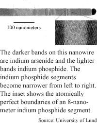
The Lund University researchers made 40-nanometer wide nanowires that have alternating segments of indium arsenide and indium phosphide. The segments of indium phosphide ranged from 100 nanometers to 1.5 nanometers long depending on the growth rate, and the thinnest indium phosphide segments had atomically perfect boundaries. "The growth rate... in our technique can be kept on the level of one atomic monolayer per second for optimal heterostructure control," said Samuelson.
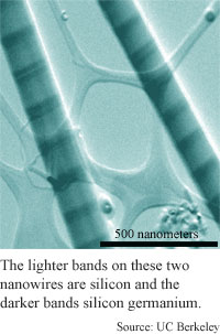
The UC Berkeley researchers made 50- to 300-nanometer wide nanowires that have alternating segments of silicon and silicon germanium.
The Harvard nanowire devices could be used for nanoscale bar codes, biological and chemical sensors and polarized LEDs in two years, said Lieber. Using the nanowires for logic circuits, photonic and electronic waveguide and lasers is likely to take at least five years, he said.
The Lund University nanowire devices could be used as scanning probe tips within a few years, said Samuelson. They could be used as single photon sources in five years, he said.
The UC Berkeley nanowire devices could be used as light sources and in thermoelectric applications like keeping electronic devices cool and turning heat into electricity in five to ten years, said Yang.
Lieber's research colleagues were Mark Gudiksen, Lincoln Lauhon, Jianfang Wang and David Smith of Harvard University. They published their results in the February 7, 2002 issue of the journal Nature. Their research was funded by the Air Force Office of Scientific Research (AFOSR), the Defense Advanced Research Projects Agency (DARPA) and the Office of Naval Research (ONR).
Samuelson's research colleagues were Mikael Björk, Jonas Ohlsson, Torsten Sass, Ann Persson, Claes Thelander, Martin Magnusson, Knut Deppert and Reine Wallenberg of Lund University. They published their results in the February issue of the journal Nano Letters and the February 11, 2002 issue of the journal Applied Physics Letters. Their work was funded by the Swedish Foundation for Strategic Research, the Swedish Research Council, VR and the European Union.
Yang's research colleagues were Yiying Wu and Rong Fan of the University of California at Berkeley. They published their results in the February issue of Nano Letters. Their work was funded by the National Science Foundation (NSF), U.S. Department of Energy (DoE) and the University of California at Berkeley.
Timeline: 2 years; 5 years; 5-10 years
Funding: Government; University
TRN Categories: Materials Science and Engineering; Semiconductors; Nanotechnology; Integrated Circuits
Story Type: News
Related Elements: Technical paper "Growth of nanowire superlattice structures for nanoscale photonics and electronics," Nature, February 7, 2002; Technical paper "One-dimensional Steeplechase for Electrons Realized," Nano Letters, February, 2002; Technical paper "One-dimensional heterostructures in semiconductor nanowhiskers," Applied Physics Letters, February 11, 2002; Technical paper "Block-by-Block Growth of Single-Crystalline Si/SiGe Superlattice Nanowires," Nano Letters, February, 2002
Advertisements:
February 13, 2002
Page One
Tiny wires turn chips inside out
Cooperative robots share the load
Nanotubes take tiny temperatures
Nanotech scheme envisions DNA origami
Electric switch flips atoms
News:
Research News Roundup
Research Watch blog
Features:
View from the High Ground Q&A
How It Works
RSS Feeds:
News
Ad links:
Buy an ad link
| Advertisements:
|
 |
Ad links: Clear History
Buy an ad link
|
TRN
Newswire and Headline Feeds for Web sites
|
© Copyright Technology Research News, LLC 2000-2006. All rights reserved.