Stamps
bang out silicon lines
By
Eric Smalley,
Technology Research NewsPeople have been pressing stamps into wet clay, soft wax and thin sheets of gold for thousands of years. Researchers at Princeton University have found a way to do the same with the wafers of silicon used to make computer chips, opening the way for this ancient technique to become the future of chipmaking.
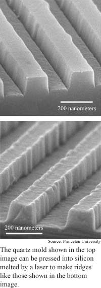
The researchers' laser-assisted direct imprint (LADI) process uses a laser to melt microscopically thin layers of silicon, then presses a quartz mold into the molten silicon. Removing the mold from the cooled, re-solidified silicon leaves a precise imprint in the wafer.
The process takes less than one millionth of a second and can be used to create surface structures smaller than 10 nanometers. The high speed and ability to produce fine features make the process a promising candidate to replace today's minutes-long, more expensive, multistep photolithography chipmaking process, which uses light and chemicals to etch lines as thin as 65 nanometers into silicon. A nanometer is one millionth of a millimeter and 10 nanometers is the width of 100 hydrogen atoms.
"What distinguishes LADI from photolithography is its sub-10 nanometer resolution, its high speed and high-throughput processing, and its ability to directly pattern without the use of a [photo]resist or etching," said Chris Keimel, a researcher at Princeton.
The researchers produced prototype patterns in silicon by etching microscopic lines and squares into one-millimeter-thick blocks of quartz, then pressing the blocks against the surface of silicon wafers and firing finely tuned ultraviolet laser pulses through the quartz molds. Quartz is transparent to the particular 308-nanometer wavelength ultraviolet light the researchers used, but silicon absorbs this wavelength and, as a result, heats up.
As the silicon wafers melted to a depth of about 280 nanometers, the liquid silicon rapidly filled the gaps in the mold. The researchers imprinted two patterns in silicon: a series of ridges 140 nanometers wide and 110 nanometers high, and raised squares 110 nanometers high and 8,000 nanometers on a side.
The researchers found 10-nanometer wide lines on the edges of the ridges formed by slight trenches in the corners of one of the molds, which proves that the process can eventually be used to make features smaller than are achievable using photolithography, said Keimel.
The process is quick because molten silicon flows with three times less resistance than water, which allows it to rapidly fill very small spaces.
The process could also be used to pattern other materials used in computer chips, said Keimel. Patterning computer chips' many layers of metals, semiconductors and insulators this way would require multiple lasers because different materials melt in different kinds of light. "Different materials absorb different wavelengths of light, so the laser source and material to be imprinted would need to be matched," he said.
Any fast, cheap process for producing computer chips has the potential to replace today's costly photolithography process, said Tsu-Jae King, an associate professor of electrical engineering and computer sciences at the University of California at Berkeley. "Lithography [is] the bottleneck in terms of cost and throughput for manufacturing integrated circuits," she said.
In theory, LADI could be used to form the tricky gate electrode layer in integrated circuits, said King. Gate electrodes are the silicon switches that turn transistors on and off, and getting their size and alignment right is critical in chipmaking, she said.
If the researchers' process can form new features in precise alignment with existing features on a silicon wafer, "then it should become a compelling choice for critical-layer patterning in integrated circuit manufacturing," said King. The process produces chip structures "at much lower cost than present-day optical lithography," she said.
LADI could be used for practical applications in three to five years, said Keimel. The researchers' next steps are to extend the technique to other materials and to apply it to large surfaces by moving the mold or surface regular intervals and repeating the stamping process, he said.
Keimel's research colleagues were Stephen Chou and Jian Gu, of Princeton University. They published the research in the June 20, 2002 issue of the journal Nature. The research was funded by the Defense Advanced Research Projects Agency (DARPA), the Office of Naval Research (ONR) and the Army Research Office (ARO).
Timeline: 3-5 years
Funding: Government
TRN Categories: Integrated Circuits, Semiconductors
Story Type: News
Related Elements: Technical paper, "Ultrafast and direct imprint of nanostructures in silicon," Nature, June 20, 2002
Advertisements:
June 26/July 3, 2002
Page One
PCs augment reality
Stamps bang out tiny silicon lines
Bent wires make cheap circuits
Mixes make tiniest transistors
Plastic computer memory advances
News:
Research News Roundup
Research Watch blog
Features:
View from the High Ground Q&A
How It Works
RSS Feeds:
News
Ad links:
Buy an ad link
| Advertisements:
|
 |
Ad links: Clear History
Buy an ad link
|
TRN
Newswire and Headline Feeds for Web sites
|
© Copyright Technology Research News, LLC 2000-2006. All rights reserved.