Nanotubes
grown in place
By
Eric Smalley,
Technology Research NewsResearch in recent years has generated a lot of excitement about carbon nanotubes, those infinitesimal tubes formed of carbon sheets a mere one atom thick. The more researchers find out about them, it seems, the more potential uses they gain.
Nanotubes are extraordinarily strong, conduct electricity, vibrate at high frequencies, emit light, and are sensitive to the presence of minute amounts of substances.
But there's a lot of hard work to be done before the average person routinely uses devices that contain nanotubes. Getting the thread-like molecules to form in specific places, for instance, is a formidable challenge.
Stanford University researchers have made this easier with a method for growing individual tubes directly between pairs of electrodes. The researchers built arrays of metal electrodes, then coaxed nanotubes to form, suspended, in the gaps between them, said Hongjie Dai, an assistant professor of chemistry at Stanford.
The technique could be used to produce several types of electronic components, said Dai. Nanotubes' microscopic size and very long, thin shape mean they are able to vibrate extremely rapidly, and rapidly vibrating nanotubes are sensitive to subtle changes.
This ability could make them useful as sensors that measure forces like acceleration, and for tuning radio waves in communications devices. They could be used in chemical sensors; strain gauges; electromechanical transducers, which convert sound, pressure or light to electrical signals; and high frequency mechanical resonators for telecommunications applications like cell phones, according to Dai.
A common laboratory method for producing nanotubes, which occur naturally in small amounts in soot, is to cause carbon to condense out of a hot vapor of chemicals. It is difficult, however, to use this method to get nanotubes to grow in the specific locations and orientations needed to form electrical components.
In contrast, the Stanford method allowed the nanotubes to form between metal electrodes the researchers had added to a silicon wafer using photolithography, the process of etching materials with light and chemicals that is used to make computer chips.
The resulting nanotubes were 2.5 nanometers in diameter and spanned electrode gaps ranging from 3,000 to 10,000 nanometers. A nanometer is one millionth of a millimeter. The longest of the nanotubes were as long as the width of two red blood cells, but were 2,000 times narrower than a single red blood cell.
The researchers used the metal molybdenum for the electrodes and added small amounts of iron to encourage the nanotube growth process. They found that molybdenum both survived the high-temperature nanotube growth process and did not inhibit nanotube growth, according to Dai. Using the metals gold, titanium, tantalum or tungsten resulted either in faulty electrodes or no nanotubes.
The researchers were able to get single nanotubes to form between electrodes 30 percent of the time, and were able to get multiple nanotubes to span the gaps 90 percent of the time, according to Dai.
Some of the suspended nanotubes worked as transistors, which control the flow of electricity in computer chips. The suspended nanotube transistors were comparable to those grown on flat surfaces using more common techniques, according to Dai.
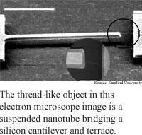
The researchers also used a nanotube to electrically connect a cantilever to a silicon surface. Making a precise connection between a nanotube and a moving part allowed the researchers to test the nanotubes' electromechanical properties, said Dai. For instance, the researchers found that a nanotube's resistance to the flow of electricity increased when they stretched it, he said.
The work is important because it allows researchers to grow nanotubes directly in electrical and electromechanical devices, said Paul McEuen, a physics professor at Cornell University. "You can grow them where you want them." Other approaches to integrating nanotubes and electronics involve processing steps that occur after the nanotube are grown, which can damage the nanotubes, he said.
The researchers' technique could be used in practical applications in two to five years, said Dai. The next steps in their research are carrying out studies of the tubes' basic electromechanical properties studies and making nanoelectromechanical devices, he said.
Dai's research colleagues were Nathan Franklin, Qian Wang, Thomas Tombler, Ali Javey and Moonsub Shim. They published the research in the July 29, 2002 issue of Applied Physics Letters. The research was funded by the Defense Advanced Research Projects Agency (DARPA), the Semiconductor Industry Association, The David and Lucile Packard Foundation, and the Alfred P. Sloan Foundation.
Timeline: 2-5 years
Funding: Government, Corporate, Private
TRN Categories: Chemistry; Integrated Circuits; Materials Science and Engineering; Nanotechnology
Story Type: News
Related Elements: Technical paper, "Integration of suspended carbon nanotube arrays into electronic devices and electromechanical systems," Applied Physics Letters, July 29, 2002
Advertisements:
August 7/14, 2002
Page One
Ultimate memory demoed
Programming tool makes bugs sing
Nanotubes grown in place
Quantum secrets ride phone lines
Chip keeps atoms in line
News:
Research News Roundup
Research Watch blog
Features:
View from the High Ground Q&A
How It Works
RSS Feeds:
News
Ad links:
Buy an ad link
| Advertisements:
|
 |
Ad links: Clear History
Buy an ad link
|
TRN
Newswire and Headline Feeds for Web sites
|
© Copyright Technology Research News, LLC 2000-2006. All rights reserved.