Nanoscale
LED debuts
By
Kimberly Patch,
Technology Research NewsBecause high-speed communications are carried out using light pulses, the industry is always on the lookout for small, efficient light sources. At the same time, a key need of the emerging quantum cryptography market, which promises to provide perfectly secure communications, is a light source that can reliably mete out single photons.
A group of researchers from Switzerland have found a way to make extremely small light-emitting diodes that could provide optical communications with a smaller, low-power light source. The method could also lead to diodes so small they could be single-photon sources.
Key to producing the devices was figuring out how to construct and align such small electrical components, according to Andrea Fiore, an assistant professor at The Swiss Federal Institute of Technology at Lausanne (EPFL) and a researcher at the Italian National Research Council (CNR).
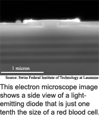
The researchers modified a method used to make a type of laser from semiconductor chip material. The method is usually used to fabricate devices with active electrical-optical areas of two or three microns, which is about half the size of a red blood cell. The researchers' modifications allowed them to produce a device with an active area of 100 nanometers, or about one 50th the size of a red blood cell. The entire device measures 600 nanometers across. A nanometer is one thousandth of a micron and one millionth of a millimeter.
The goal was to make a device that directed current to a layer containing quantum dots -- 25-nanometer-wide, seven-nanometer-high bits of the semiconductor indium arsenide. Quantum dots can confine single, negatively-charged electrons. When an electric current brings a positively-charged hole to the dot, the electron and hole combine to emit a photon.
The difficult part was producing a device that efficiently guided electricity to the tiny quantum dots, said Fiore. There were two problems to solve, she said. The first was finding an efficient way to align the device's electrical contacts, and the second was finding a way to confine the electrical flow to a specific, vertical path within the device.
The researchers used optical lithography to etch mesas one or two microns in diameter into a cap of the semiconductor gallium arsenide attached to a layer of aluminum-gallium arsenide on top of the device. Then they heated the sample to 400 degrees Celsius and exposed it to water vapor, which caused the aluminum in the layer below the cap to oxidize, or combine with some of the oxygen in the water. This is the same type of reaction that causes iron to rust.
The oxidation continued underneath the gallium arsenide cap, spreading from the outside in, said Fiore. The researchers timed the oxidation process to leave a narrow channel of unoxidized material under the center of the cap. "Since the oxide is insulating, this defines a current constriction, which can be made much smaller than the original gallium arsenide mesa," said Fiore.
This resulted in an automatic alignment of the contact area -- the mesa. This solved the first problem: because the contact area was already lined up, less precision was required in depositing metal electrodes onto the contact. Otherwise, "having to align such small structures [would require] high-resolution fabrication tools, which are expensive and not compatible with an industrial process," Fiore said.
The researchers then attached metal contact layers above the mesa and below the base. "Because the surface is covered with insulating aluminum oxide everywhere except on the gallium arsenide mesas, current can flow only inside the [channel] in the aluminum gallium arsenide layer," Fiore said.
The researchers solved the challenge of confining the current by working with the physical design of the chip, said Fiore. In the researchers' first attempt to make the devices, the electrical current spread laterally rather than being channeled to the quantum dots, said Fiore. "In order to avoid that, we carefully redesigned the layer above the quantum dots [to make] it easier for the current to flow vertically than laterally," she said.
The researchers' quantum dots turned out to be very temperature-tolerant, meaning they continue to confine electrons even when the temperature rises to room temperature. "This holds true only as long as the energy barrier to [electron] escape is larger than the thermal energy. For most quantum dots this is not true anymore at room temperature," said Fiore.
The researchers' tiny light emitting diode produces infrared light with a wavelength of 1.3 microns, which is widely used in today's fiber-optic communications. Its small size makes the device useful as a light source for single-mode fiber, according to Fiore. Single mode fibers are 8 to 9 microns in diameter, and are used for long, high-speed links.
The devices could eventually be scaled down so that they contain single quantum dots, which would only emit one photon at a time, said Fiore. Single-quantum-dot light emitting diodes could "produce light pulses containing single photons, and this [could] be used to transmit information in a quantum-secure way," Fiore said.
Quantum cryptography, which has the potential to produce perfectly secure communications, is just emerging as a commercial product. Quantum cryptography devices use states of photons -- like the way a photon is polarized -- to represent the ones and zeros of computing. A series of photons representing a string of ones and zeros is used as a key to encrypt and decrypt data.
Single photon pulses cannot be observed without altering their states. Therefore, it is possible to tell for sure whether a cryptographic key represented by the quantum states of a string of single photons has been compromised. Eavesdropping on a single-photon transmission will alter the photon's state.
The quantum dot diode shows promise as a better source of single photons than the devices currently in use. Current quantum cryptography systems use heavily-filtered lasers, which mostly produce empty pulses, sometimes produce single pulses, and occasionally produce two-photon pulses. Existing quantum dot single-photon sources are relatively inefficient and work only at cryogenic temperatures.
The researchers' device is remarkably efficient, and cleverly made, said Pablo Vaccaro, a senior researcher at Adaptive Communications Research Laboratories (ATR) in Japan. The researchers "applied in a clever way the wet oxidation technique already in use," he said.
The research is novel "from the point of view that it demonstrates the fabrication of sub-micron size LEDs, each one with an active region that contains a few tens or a few hundreds of quantum dots each," said Vaccaro. The technique could be refined to eventually produce single quantum dot devices, he added.
The current, multiple-quantum-dot design could be used in very short optical links like those within computer chips, Vaccaro said.
The researchers are working on further scaling down the diode to produce a device that emits single photons from single quantum dots at room temperature, said Fiore. The researchers are also working on making the device more efficient, she said. "We now want to further scale down the LED to a size where emission from a single quantum dot can be isolated," she said. "Another major objective is... optimizing the carrier-photon interaction to maximize the LED efficiency."
The method could produce practical, single-photon devices in two to three years, Fiore said.
Fiore's research colleagues were Jianxin X. Chen and Marc Ilegems of The Swiss Federal Institute of Technology at Lausanne. They published the research in the September 2, 2002 issue of Applied Physics Letters. The research was funded by the European Union and the Swiss National Science Foundation.
Timeline: 2-3 years
Funding: Government
TRN Categories: Materials Science and Engineering; Optical Computing, Optoelectronics and Photonics; Physics; Quantum Computing and Communications
Story Type: News
Related Elements: Technical paper, "Scaling Quantum-Dot Light-Emitting Diodes to Submicrometer Sizes," Applied Physics Letters, September 2, 2002.
Advertisements:
October 30/November 6, 2002
Page One
Nanoscale LED debuts
Data transfer demo sets speed mark
Pulling nanotubes makes thread
Text software spots intruders
Microwave drill melts concrete
News:
Research News Roundup
Research Watch blog
Features:
View from the High Ground Q&A
How It Works
RSS Feeds:
News
Ad links:
Buy an ad link
| Advertisements:
|
 |
Ad links: Clear History
Buy an ad link
|
TRN
Newswire and Headline Feeds for Web sites
|
© Copyright Technology Research News, LLC 2000-2006. All rights reserved.