Chemicals map nanowire arrays
By
Eric Smalley,
Technology Research NewsWith today's chipmaking technologies likely to reach physical limits in the next decade or so, researchers have been working on alternative approaches to making smaller computer circuits.
One promising possibility is arrays of nanowires whose junctions form tiny, densely packed transistors. Transistors are electrical switches that are the building blocks of computer chips. Nanowires measuring a few nanometers in diameter could enable computer chips that pack a trillion transistors per square centimeter, which is several orders of magnitude more than current chipmaking technologies are likely to achieve. A nanometer is one millionth of a millimeter.
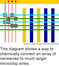
The tiny arrays must also connect to the larger circuits of electronic devices like computers. It is a challenge, however, to switch specific transistors on and off within a group of several thousand of the tiny wires using a relatively small number of control wires required to make the connection to larger circuits.
Researchers at Harvard University and the California Institute of Technology have come up with a scheme to chemically modify selected nanowire junctions to make them react differently to electrical current than the junctions around them.
The chemical modification makes cross points more sensitive to switching voltage than unmodified cross points, said Charles Lieber, a professor of chemistry at Harvard. "[It] enables us to introduce a coding scheme within the array so that we can selectively address the output nanowires," he said. This provides a means of bridging the nano and micro worlds, he added.
Transistors have three terminals: source, drain and gate. Current flows from the source to the drain and is controlled by the gate. When a voltage is applied to the gate, its electric field makes the channel between the source and drain more conductive, which allows current to flow. An input signal opens the gate, switching the transistor on to create an output signal.
In a transistor made from crossed nanowires, one nanowire is the channel and the perpendicular nanowire is the gate. In an array of nanowire transistors, each gate, or input, nanowire crosses every channel, or output, nanowire, making every input affect every output.
The researchers showed that chemically modifying a diagonal line of junctions -- input one and output one, input two and output two, input three and output three, and input four and output four -- in an array of 16 junctions formed from four input wires and four output wires makes those four transistors individually addressable.
Chemically modifying the junctions in more complicated patterns would make it possible to address a set of transistors using a smaller number of input wires, said Lieber. Modifying the right junctions makes it possible to individually control 24 transistors using four input wires, for example. This makes it practical to connect a nanowire array to ordinary-size circuits.
The researchers' scheme is the second major effort aimed at making nanowire arrays addressable. In 2001, Hewlett-Packard Laboratories developed a method of addressing individual junctions in a nanowire array memory device. The HP addressing scheme calls for randomly sprinkling gold nanoparticles on the portions of the nanowires that extend beyond the junctions, then overlaying these portions of the nanowires with larger control wires.
With the right concentration of nanoparticles, half of the junctions between the control wires and nanowires are connected by nanoparticles. A connection represents 1 and no connection represents 0. Mapping the sequence of control wires that a nanowire is connected to yields a unique binary number. Addressing two perpendicular nanowires by their unique binary numbers addresses the junction of the two wires. (See "HP maps molecular memory," TRN July 18, 2001)
The Harvard/Caltech technique has two advantages over the HP approach, according to Lieber. First, each HP device is unique, and its code has to be determined by testing each nanowire, which takes time and resources, he said. Second, the junctions in the HP device are diodes rather than transistors. Transistors provide signal gain, meaning the output voltage is higher than the input voltage. Because electrical signals fade, signal gain is necessary to allow signals to propagate through circuits.
The researchers are working to integrate the address decoder with nanoscale memory arrays, said Lieber. "This is required for realizing a true nano memory chip," he said. It is also a step towards the integrated memory and logic needed to make a functional nanocomputer, he said.
Prototype memory and processors could be built within two to five years, and commercial devices within five to ten years, said Lieber.
Lieber's research colleagues were Zhaohui Zhong, Deli Wang and Yi Cui of Harvard and Marc W. Bockrath of the California Institute of Technology. They published the research in the November 21, 2003 issue of Science. The research was funded by the Defense Advanced Research Projects Agency (DARPA).
Timeline: 5-10 years
Funding: Government
TRN Categories: Nanotechnology; Integrated Circuits
Story Type: News
Related Elements: Technical paper, "Nanowire Crossbar Arrays as Address Decoders for Integrated Nanosystems," Science, November 21, 2003
Advertisements:
January 28/February 4, 2004
Page One
Robot automates science
Chemicals map nanowire arrays
Badge controls displays
Neural-chaos team boosts security
Briefs:
Inkjet goes 3D
Nanotubes tied to silicon circuit
Micro tweezers have ice grip
Nanorings promise big memory
Protein orders semiconductor bits
Technique detects quantum state
News:
Research News Roundup
Research Watch blog
Features:
View from the High Ground Q&A
How It Works
RSS Feeds:
News
Ad links:
Buy an ad link
| Advertisements:
|
 |
Ad links: Clear History
Buy an ad link
|
TRN
Newswire and Headline Feeds for Web sites
|
© Copyright Technology Research News, LLC 2000-2006. All rights reserved.