Photonic chips go 3D
By
Eric Smalley,
Technology Research NewsThe dream of building computer chips that use light signals rather than electricity has entered the realm of serious research in recent years with the advent of photonic crystal, a material that blocks and channels light within extremely small spaces.
Producing practical photonic crystal chips, however, includes several challenges: making three-dimensional devices that emit light from specific points, emit at the wavelengths used by today's optical telecommunications equipment and can be manufactured using processes suited to mass production.
Research teams from the Massachusetts Institute of Technology and from Kyoto University have made devices that meet all three challenges.
The techniques could be used to make smaller, more efficient communications devices; create optical memory and quantum computing and communications devices; develop new types of lasers and biological and chemical sensors; and could ultimately lead to all-optical computer processors.
The semiconductor industry took off with the advent of a practical and low-cost method of integrating a large number of transistors into a single chip, said Minghao Qi, a research assistant at MIT. "It is natural then to envision the possibility of integrated photonics, where information is processed fully in the optical domain [at the high] bandwidth of photons," he said.
Photonic crystal is usually made from the same semiconductor materials as computer chips using common chipmaking techniques like photolithography. It contains regularly spaced gaps of air or other materials that form boundaries within the crystal that refract, or bend, specific wavelengths of light. Refraction is responsible for the illusion that a drinking straw bends at the air-liquid boundary. Portions of the materials that do not contain gaps channel light within the crystal and emit light from it.
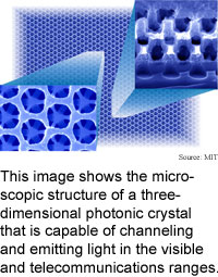
The MIT photonic chip has seven layers that each contain two types of two-dimensional photonic crystal. One type is an arrangement of rods surrounded by air and the other type is solid material perforated with air holes. The rod slab is positioned above the hole slab in each layer, and the layers are offset to produce steps. The holes are about 500 nanometers in diameter, or about one-tenth the size of a red blood cell. The material blocks light at wavelengths of 1.3, 1.4 and 1.5 microns. Telecommunications systems use near-infrared 1.3- and 1.55-micron wavelengths.
The researchers filled specific air holes and gaps between rods during the manufacturing process to create solid areas, or defects, that emit light. "A critical goal in photonic crystal [research] is the ability to put arbitrary defects with precisely controlled shapes and sizes at designed locations," said Qi.
The two types of two-dimensional photonic crystal in each layer of the three-dimensional crystal also allow for polarization control, said Qi. A light beam's electric field is ordinarily oriented in a plane perpendicular to the beam. The electric field of polarized light is confined to one direction within the plane. Controlling polarization is important because transferring light signals from photonic crystal to optical fibers requires matching the polarizations of the devices, he said.
The crystal is more efficient than previous three-dimensional photonic crystals, and the seven layers can be formed in four processing steps, said Qi.
The Kyoto University team has advanced its existing woodpile-structured three-dimensional photonic crystal with a method to make solid areas in specific locations and have shown that the material precisely controlled light, said Susumu Noda, a professor of electronic science and engineering at Kyoto University.
The woodpile photonic crystal consists of perpendicular layers of semiconductor rods. The researchers' design calls for 200-nanometer-wide rods spaced 700 nanometers center to center. The photonic crystal controls 1.55-micron light.
The researchers also sandwiched a light source inside their photonic crystal, which is a step toward fully integrated optical devices, said Noda.
The MIT process could be used to make practical telecommunications devices and biological and chemical sensors in two to three years, said Qi. High-quality devices that could be coupled to optical fiber could take five years, he said. Simple all-optical computer chips could take 10 years to develop, he said.
Devices based on the Kyoto method could become practical in five to ten years, said Susumu.
Qi's research colleagues were Elefterios Lidorikis, Peter Rakich, Stephen Johnson, John Joannopoulos, Erich Ippen and Henry Smith. The work appeared in the June 3, 2004 issue of Nature. The research was funded by the National Science Foundation (NSF).
Susumu's research colleagues were Shinpei Ogawa, Masahiro Imada, Susumu Yoshimoto and Makoto Okano. The work appeared in the June 3, 2004 issue of Sciencexpress. The research was funded by Core Research for Evolution Science and Technology (CREST), Japan Science and Technology Agency (JST), and the Ministry of Education, Culture, Sports, Science and Technology (MEXT) of Japan.
Timeline: 2-3 years, 5 years, 7-8 years, 10 years
Funding: Government, Corporate
TRN Categories: Optical Computing, Optoelectronics and Photonics; Materials Science and Engineering
Story Type: News
Related Elements: Technical paper, "Control of Light Emission by 3D Photonic Crystals", Sciencexpress, June 3, 2004; technical paper, "A Three-dimensional Optical Photonic Crystal with Design Point Defects," Nature, June 3, 2004
Advertisements:
July 28/August 4, 2004
Page One
Photonic chips go 3D
Online popularity tracked
Summarizer gets the idea
Electric fields assemble devices
Briefs:
Process prints silicon on plastic
Tool automates photomontage edits
Device promises microwave surgery
Hologram makes fast laser tweezer
Chemistry yields DNA fossils
Particle chains make quantum wires
News:
Research News Roundup
Research Watch blog
Features:
View from the High Ground Q&A
How It Works
RSS Feeds:
News
Ad links:
Buy an ad link
| Advertisements:
|
 |
Ad links: Clear History
Buy an ad link
|
TRN
Newswire and Headline Feeds for Web sites
|
© Copyright Technology Research News, LLC 2000-2006. All rights reserved.