Molecules positioned on silicon
Researchers from Northwestern University
have demonstrated a fabrication process that allows them to pattern molecular
structures consisting of more than one type of molecule on silicon surfaces
with atomic precision.
The process, dubbed multi-step feedback control lithography, allows
for single molecule control in all three spatial directions at room temperature,
according to the researchers.
The method could be used to construct prototype molecular electronic
devices for future technologies in areas like consumer electronics and
biomedical diagnostics.
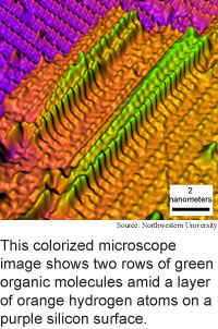
Scientists have previously demonstrated that coating a silicon
surface with a single layer of hydrogen atoms, removing one of the atoms
with a scanning tunneling microscope, and exposing the surface to styrene
molecules causes one of the molecules to attach at the site of the missing
hydrogen atom. When it attaches, the molecule removes an adjacent hydrogen
atom, which sparks a chain reaction that yields a single-molecule-wide
line of styrene on the silicon.
The Northwestern researchers have found a way to use another molecule
to confine the styrene reactions and cause styrene reactions to reverse
direction to produce double-wide lines. The technique should be compatible
with a wide range organic molecules, according to the researchers.
The researchers are working on ways to speed up the process. The
current setup is capable of constructing devices, but is too slow and
expensive to be commercially viable. One way to overcome this problem
is to use a large array of scanning tunneling microscope tips working
in parallel, according to the researchers.
The molecular fabrication process could be used practically in
10 to 20 years, according to the researchers. The work appeared in the
September 27, 2004 issue of Applied Physics Letters.
Biochip spots single viruses
Cooler material boosts fuel cells
Pen stroke cuts PDA Web clutter
Wide laser makes simple tweezers
Briefs:
Biochip levitates droplets
Nanotubes form transparent film
Molecules positioned on silicon
Mechanical valve design goes nano
Angles increase optical storage
Crystal links ultraviolet photons
Research Watch blog
View from the High Ground Q&A
How It Works
RSS Feeds:
News
Ad links:
Buy an ad link
Ad links: Clear History
Buy an ad link
|
TRN
Newswire and Headline Feeds for Web sites
|
© Copyright Technology Research News, LLC 2000-2010. All rights reserved.