Nano bridge builds logic
By
Eric Smalley,
Technology Research NewsResearchers from the Japanese National Institute for Materials Science have given an old technology -- the mechanical electric switch -- a quantum update.
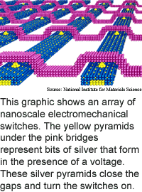
The researchers have devised a nanoscale mechanical switch that works by rapidly creating and destroying a minuscule metal bridge between a pair of wires positioned just one nanometer apart. A nanometer is one millionth of a millimeter, or the span of 10 hydrogen atoms.
The researchers' device, dubbed the quantized conductance atomic switch, could one day be used to form electronic circuits and memory devices, and could be manufactured on silicon computer chips, said Hasegawa.
Unlike earlier generations of mechanical switches, the device does not have moving parts. "Our switch works by simply applying... voltage, same as semiconductor devices," said Tsuyoshi Hasegawa, an associate director at the National Institute for Materials Science in Japan.
The atomic bridge between wires grows in the presence of a low positive voltage and shrinks in the presence of a low negative voltage. It works in a dry environment at room temperature, Hasegawa said.
The researchers' prototype switches between on and off states at 1 megahertz, or million times per second, using a voltage of 600 millivolts, or thousandths of a volt. With thinner wires, the switching speed could reach 1 gigahertz, or billion times per second, which is comparable to the switching speed of today's computer chips, said Hasegawa.
The researchers made the switch by depositing a 1-nanometer thick layer of silver on a silver sulfide-coated silver wire, positioning a platinum wire on the silver layer, and applying a negative voltage. The voltage caused the atoms in the silver layer to be incorporated into the silver sulfide coating, leaving a one-nanometer gap between the silver sulfide and platinum wires.
A positive voltage turns the switch on because it draws enough silver atoms to the surface of the silver sulfide to bridge the gap between the two wires. A subsequent negative voltage causes the silver atoms to return to the silver sulfide.
Many switches can be packed into a small area by positioning the silver sulfide wires perpendicular to the platinum wires. If each switch were used as a memory element, such a configuration would allow a memory chip made from the switches to store 2.5 gigabits per square centimeter, according to Hasegawa. Today's state-of-the-art memory chips store about 1 gigabit per square centimeter. Smaller wires would yield even higher capacities, said Hasegawa.
Because the switches are so tiny, they operate in the realm of quantum physics, which opens the possibility of using the switch to make a multi-bit memory device, according to Hasegawa. In the realm of atoms and subatomic particles, the rules of physics are different from the everyday world. Unlike that of larger switches, the electrical conductance through the researchers' tiny switch is quantized, meaning it increases or decreases by discrete amounts. A pair of the switches can represent as many as 16 values, or 4 bits, according to Hasegawa.
The researchers also used the switches to form the basic binary logic gates required to make computer processor chips. They made an AND gate using two switches formed from a single silver sulfide wire and two platinum wires combined with a resistor that restricts electric currents to specific voltages. An AND gate produces a 1 only if both inputs are 1. They made an OR gate using two switches formed from two silver sulfide wires and a single platinum wire combined with a resistor. An OR gate produces a 0 only if both inputs are 0. They made a NOT gate using one switch combined with two resistors and a capacitor, which briefly stores electric charge. A NOT gate turns an input of 1 into 0 and vice versa.
The researchers' next step is to make the switch more reliable and to develop practical methods of fabricating large numbers of the devices, according to Hasegawa.
The switch could be used in commercial products within ten years, according to the researchers.
Hasegawa's research colleagues were Kazuya Terabe of the Japanese National Institute for Materials Science and the Japan Science and Technology Agency, and Tomonobu Nakayama and Masakazu Aono of the Japanese Nation Materials Science, Japan Science and Technology Agency, and Riken. The work appeared in the January 6, 2005 issue of Nature. It was funded by the Japanese Ministry of Education, Culture, Sports, Science and Technology.
Timeline: 10 years
Funding: Government
TRN Categories: Integrated Circuits; Nanotechnology
Story Type: News
Related Elements: Technical paper, "Quantized Conductance Atomic Switch," Nature, January 6, 2005
Advertisements:
January 26/February 2, 2005
Page One
Nano bridge builds logic
Braille display drives biochip
Adaptive lights organize traffic
Nanotechnology: the physics of the very small
Briefs:
Spray-on photocells harvest infrared
Oil and water drive display
Chemical fuse makes cheap sensors
Metals speed transparent circuits
Plastic records infrared light
Magnetic logic becomes practical
Plastic memory retains data
News:
Research News Roundup
Research Watch blog
Features:
View from the High Ground Q&A
How It Works
RSS Feeds:
News
Ad links:
Buy an ad link
| Advertisements:
|
 |
Ad links: Clear History
Buy an ad link
|
TRN
Newswire and Headline Feeds for Web sites
|
© Copyright Technology Research News, LLC 2000-2006. All rights reserved.