Etching process points to nanotech production
By Ted Smalley Bowen, Technology Research NewsManufacturing at the atomic scale could be on the verge of its own mini-industrial revolution. Getting minute mass production underway, however, means moving from today's laboratory techniques to processes that can produce tiny features en mass.
Volume production is possible for objects as small as the 40 million or so transistors that make up a computer chip, but the etching processes like photolithography that are used to make them are only so precise.
Photolithography has a practical limit of about half the wavelength of the light used in the process, making it difficult to produce features smaller than 100 nanometers. To date, any mass production techniques for etching, which use a solvent to remove surface material to form patterns or shapes, can't make features smaller.
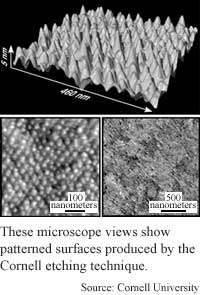
A group of researchers at Cornell have developed an etching process that can yield regular structures with features as closely spaced as 38 nanometers. A nanometer is one millionth of a millimeter, or about 10 carbon atoms long.
The process produces simple patterned surfaces, but these bumps could serve as foundations for more complicated structures. The work could contribute to the development of mass-production techniques for making small-scale lattices and forms, individual parts, or, eventually, tiny circuits and machines.
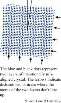
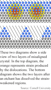
The method involves bonding skewed, single-crystal layers of silicon. The misalignment causes weak atomic bonds to form in places where the atoms of the two layers are not matched. These dislocations, or linear defects form within the bonded silicon and along its edges. The researchers then apply an etchant, or etching solution to the surface material, which dissolves the dislocations, leaving tiny bumps.
The key to the process is the etching solution, which is attracted to the dislocations. "People have used etchants made of these materials before, but really the whole key to this was developing an etchant of the right material [that dissolved the silicon] for exactly the right length of time," said Melissa A. Hines, associate professor of chemistry and chemical biology at Cornell.
To demonstrate the process, the researchers fabricated a silicon surface with bumps five nanometers high, 26 nanometers across and spaced an average of 38 nanometers apart.
The technique can theoretically be used to form topologies with regularly spaced features separated by as little as 2 nanometers, said Hines. But in order to view features and spacing that small, the researchers need to boost the magnification of their atomic force microscopy by fitting the microscope tips with carbon nanotubes, she said.
For comparison, the gap between binding sites on human antibodies is about 10 nanometers, and the size of atomic bonds is about 2 nanometers.
The work also yielded findings that countered theoretical predictions of where and how quickly the selective etching should take place.
"The etchant that we used attacks dislocations, or these regions of poor bonding, and there's been a long-standing argument that the reason the etchants preferentially eat these dislocations has to do with the strain energy," Hines said. Strain energy refers to the degree to which the bonds between the silicon wafers have been stretched or compressed by the twisting.
Earlier work has correlated strain energy with etch rate. According to Hines, however, the actual process is more complicated. "As a chemist, I think that that is too simplistic of a view. You can't just say that this bond has been stretched by X amount, therefore its reactivity goes up by Y. It depends on how you stretch it, what direction you stretch it," she said.
Rather than acting at different rates on the edge dislocations and those within the sandwiched wafers, as the theories suggested, the etch rates in the researchers' experiments were fairly consistent, according to Hines.
Instead of strain energy, it could be the chemical structure of dislocations that primarily determines etch rate, she said. "[But] to really understand what's going on here, we need to understand the structure of the dislocation - how the atoms really are bonded in these lines, and that's a very, very difficult problem to answer. It requires going there with atomic scale precision, and there's no technique right now that can do that."
However the etching process works, the resulting structures could be quite varied, making for many possible uses. "One thing we would like to use these little bumps for is to see if we can use them to act as preferential nucleation sites for growth, for example, if you wanted to grow quantum dots," Hines said. "Can you find materials that would selectively grow at the tops or in the channels?"
Another near-term goal is cultivating magnetic media by growing "small dots... that would be single domains," Hines said.
In addition, the etching process could allow the researchers to create such small silicon structures that the material would take on light-emitting properties, she said.
"People have found light-emitting forms of silicon before, so-called porous silicon, but we believe that this would be at least potentially easier to handle, because the porous silicon that people have used to date hasn't lasted as long because it's formed in solutions," said Hines.
Further out, the methods could be used to create infinitesimal trellises for biological molecules, or possibly to create extremely small machines, she said.
It's not clear when the methods could be used commercially, but researchers will probably use devices created by them within five years, Hines said.
"The method has the potential to generate perfectly ordered nanoscale features on large surface areas with minimal defects in a very simple and straightforward process," said Hicham Fenniri, an assistant professor of chemistry at Purdue University.
A further step, achieving functional surfaces such as circuitry or addressable features would be more difficult, but possible, he said. "Here self-assembly processes may perhaps provide the missing link to nano-fabricated functional silicon technology," he said.
Hines' research colleagues were Stephen L. Sass, Rikard A. Wind, Martin J. Murtagh, Fang Mei, and Yu Wang of Cornell. They published the work in the April 9, 2001 issue of the journal Applied Physics Letters. The research was funded by Phillip Morris USA.
Timeline: < 5 years
Funding: Corporate
TRN Categories: Nanotechnology
Story Type: News
Related Elements: Technical paper, "Fabrication of Nanoperiodic Surface Structures by Controlled Etching of Dislocations in Bicrystals," Applied Physics Letters, April 9, 2001.
Advertisements:
May 2/9, 2001
Page One
Jolts yield nanotube transistors
Simulation hints at quantum computer power
Metal makes DNA more conductive
Etching process points to nanotech production
Plastic pins DNA molecules in place
News:
Research News Roundup
Research Watch blog
Features:
View from the High Ground Q&A
How It Works
RSS Feeds:
News
Ad links:
Buy an ad link
| Advertisements:
|
 |
Ad links: Clear History
Buy an ad link
|
TRN
Newswire and Headline Feeds for Web sites
|
© Copyright Technology Research News, LLC 2000-2006. All rights reserved.