Bug-eye
lenses set up desktop chipmaking
By
Eric Smalley,
Technology Research NewsThe billion-dollar plants where computer chips are made are a lot like the elaborate facilities where spaceships are built. Imagine how cheap computers could be if chipmaking had more in common with a process as simple as desktop publishing.
Researchers at Harvard University have taken a significant step in that direction with the development of an array of microscopic lenses that can shrink a pattern more than 1,000 times.
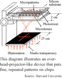
The microlens projection lithography technique uses ordinary white light shining through overhead transparencies made with a desktop printer. Current chipmaking processes involve ultraviolet lasers shining through tiny metal masks that were etched by beams of electrons.
"The microlens array in our technique forms a fly's eyes configuration that images a common pattern and produces multiple, microscale [copies of the pattern]," said Ming-Hsien Wu, a graduate student at Harvard University. The lenses are modeled after the compound eyes of insects. Each of a fruit fly's eyes, for example, is made up of about 800 separate lenses. Insects use the many separate images compound eyes provide to help detect motion or boost low-light vision.
Because the microlens process is limited to repetitive patterns, it's not likely be used to make entire computer processors, but many other chips and sections of chips used in a wide range of electronic and optical devices do have regular patterns. The technique could be used to produce transistor arrays, storage devices, sensor arrays, pixel arrays, beam splitters, optical gratings and color filters, said Wu.
Chips are ordinarily made by covering a layer of semiconductor with a protective oxide layer, then a layer of photoresist, or plastic that reacts to light. A mask outlining a pattern is positioned above the chip and light is shone through the mask. The light alters the exposed areas of the photoresist, allowing specific chemicals to wash it away along with the oxide underneath. The remaining photoresist is washed away with other chemicals, leaving the layer of oxide in the form of the mask and the layer of semiconductor exposed in the original pattern. The exposed silicon is then "doped," or altered, to become electrically conductive. Manufacturers make chips with feature sizes as small as 180 nanometers using this process.
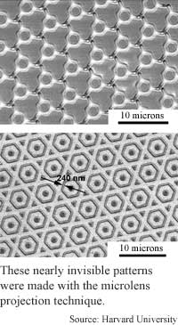
The microlens projection technique instead uses arrays of one of two types of lenses: polystyrene microspheres or convex microlenses. The researchers have produced uniform patterns on 2-square-centimeter surfaces by projecting 25-square-centimeter transparency images through arrays of microspheres 1.5 to 10 microns in diameter, said Wu.
Chips made using microspheres had chip features as small as 200 nanometers, while the similar microlense technique allowed for features as small as 400 nanometers.
Current chipmaking processes include steps that reduce pattern sizes four or five times, said Wu. The small scale of the masks and light sources used to do this make these processes sensitive, which is is one reason they are expensive. "In conventional lithography, the formation of patterns on photoresist is very sensitive to the lateral and vertical positions of the chromium masks and it requires high-precision stages to control the positions of the masks," said Wu. "The whole lithographic facility has to be placed in an environment with very low background vibration."
"In our technique, the formation of patterns on photoresist is much less sensitive to the positions of the transparency masks," said Wu. "For a 25-by-25-square-centimeter transparency mask, even a one centimeter shifting of the mask would not cause obvious change in the shape of the produced patterns," he said.
The microlens photolithography technique could be used in practical applications in two to five years, said Wu.
Wu's research colleague was George M. Whitesides. They published the research in the April 16, 2001 issue of the journal Applied Physics Letters. The research was funded by the Defense Advanced Research Projects Agency (DARPA).
Timeline: 2-5 years
Funding: Government
TRN Categories: Integrated Circuits
Story Type: News
Related Elements: Technical paper, "Fabrication of arrays of two-dimensional micropatterns using microspheres as lenses for projection photolithography," Applied Physics Letters, April 16, 2001
Advertisements:
June 6, 2001
Page One
Search scheme treads lightly
Bug-eye lenses set up desktop chipmaking
DNA parts make versatile nanotubes
Watermarks hide in plain text
Material bends sound waves
News:
Research News Roundup
Research Watch blog
Features:
View from the High Ground Q&A
How It Works
RSS Feeds:
News
Ad links:
Buy an ad link
| Advertisements:
|
 |
Ad links: Clear History
Buy an ad link
|
TRN
Newswire and Headline Feeds for Web sites
|
© Copyright Technology Research News, LLC 2000-2006. All rights reserved.