Sandia speeds microtube chip making
By Eric Smalley, Technology Research NewsResearchers at Sandia National Laboratories have developed a process for more quickly and cheaply putting networks of tiny tubes on microchips.
Sandia's room temperature, single-wafer fabrication process dramatically increases yields for making chem-labs-on-a-chip and other biological and chemical MicroElectroMechanical Systems (MEMS).
BioMEMS, which are comparable in size and appearance to integrated circuits, use tiny channels to control the flow of small amounts of gases and liquids. These microfluidic devices power the emerging class of portable laboratories that includes chemical warfare sensors, pollution detectors and DNA analyzers.
Current processes for fabricating BioMEMS involve etching matching trenches on two wafers, lining up the wafers precisely and fusing them using heat or glue. The breakthrough that enabled the single-wafer process was the invention of room temperature silicon oxynitride film deposition, according to Carolyn M. Matzke, a postdoctoral appointee at Sandia's Compound Semiconductor Research Laboratory in Albuquerque.
"This is a key process that allows us to dissolve the sacrificial polymer out from the inside of the channel in the final processing step," she said.
In standard integrated circuit fabrication, which uses single wafers, circuits are created in thin layers of silicon, which are then sandwiched between layers of an insulator. But these films of silicon are applied to the wafer at high temperatures that would destroy the polymer ridges that are critical to the Sandia process, Matzke said. The low temperatures of the process also mean that other materials that would be damaged or destroyed at high temperatures can be integrated into the devices.
The current two-wafer BioMEMS processes tend to be difficult and time-consuming, and produce yields of around 10 to 15 percent. "The materials must be thermo-mechanically matched so that under high temperatures, which chemically bond the two pieces together, one doesn't break or warp. The surfaces [must be] pristine and the wafers must be globally flat so that they make contact," Matzke said.
The single-wafer BioMEMS process developed by Matzke, Carol I. H. Ashby, Monica Bridges, Leonardo Griego and Channy Wong avoids these problems. It produces yields of around 90 to 95 percent and takes about one-third the time of the two-wafer processes, Matzke said. It is also compatible with standard integrated circuit fabrication.
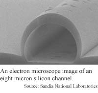
The researchers have made channels as small as eight microns in diameter on silicon wafers. The process has a lot of potential for making even smaller channels, said Marc Madou, director of the Center for Industrial Sensors and Measurements, a National Science Foundation center at Ohio State University in Columbus. "Here you might have an opportunity to make very small things, perhaps even submicron," he said.
Madou pointed out, however, that the two-wafer technology is not sitting still, either. Better bonding processes, including room temperature bonding processes, are being found there, as well," Madou said. In addition, "The whole field is moving toward plastic, and it's hard to beat plastic in terms of cost."
In the Sandia process, the researchers apply a thin layer of photoresistant polymer -- a material the changes properties when exposed to light -- to a wafer of silicon, quartz or glass. They lay a mask over the polymer and expose it to light, then use chemicals to wash away the exposed areas, leaving the unexposed areas as ridges on the surface of the wafer.
Next, the researchers heat the wafer to 100°C for 20 seconds in order to round off the edges of the ridges. They then apply a 2-micron thick film of silicon over the wafer. Last, they soak the wafer in chemicals that dissolve the remaining polymer, leaving the desired channels.
The researchers are currently integrating microvalves, pumps and a micro hot plate with the channels to build a micro protein processing plant, Matzke said. Another potential application for microfluidic channels is on-chip cooling systems for integrated circuits.
Given its compatibility with existing integrated circuit fabrication technology, the Sandia process could be used commercially within two years, according to Matzke. The research was funded by the U.S. Department of Energy. Sandia Labs was granted a patent for the process in May.
Timeline: <2 years
Funding: Government
TRN Categories: MEMS; Semiconductors and Materials
Story Type: News
Related Elements: Photo of eight micron diameter microfluidic channel
Advertisements:
June 21, 2000
Page One
Nature nurtures nanotech
Virtual physicals at hand
Sandia speeds microtube chip making
Data compression makes the heart grow fuzzy
Multicast promises lighter wireless Internet
News:
Research News Roundup
Research Watch blog
Features:
View from the High Ground Q&A
How It Works
RSS Feeds:
News
Ad links:
Buy an ad link
| Advertisements:
|
 |
Ad links: Clear History
Buy an ad link
|
TRN
Newswire and Headline Feeds for Web sites
|
© Copyright Technology Research News, LLC 2000-2006. All rights reserved.