Sandia brews cheap telecom laser
By Kimberly Patch, Technology Research NewsSandia National Laboratories researchers have modified a relatively cheap form of laser to handle long distance telecommunications, promising lower costs -- at least for carriers.
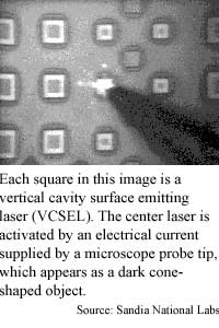
The researcher's vertical cavity surface-emitting laser (VCSEL) emits 1.3-micron lightwaves, which is the optimum frequency for medium-distance fiber-optic transmissions.
Optical fibers transmit information via bursts of light from tiny lasers, usually one to each fiber. The two types of lasers commonly used in fiber optics are VCSELs and edge emitters. Edge emitters are more difficult to manufacture and thus more expensive, but because they're able to transmit at the 1.3 micron frequency needed for medium distance fiber-optic telecommunications, they have dominated that market. VCSELs have until now only been able to emit shorter 850 nm wavelengths appropriate only for short distance fiber connections.
The 1.3 micron frequency is special because light at that wavelength travels through optical fibers at the rate of minimum dispersion, meaning with very little loss of intensity. Signal loss is not a problem in short connections, but in longer connections signal losses must eventually be corrected with signal amplifiers.
It has been obvious that a 1.3 micron VCSEL laser would be useful, but a sticky technical problem has until now stymied efforts to produce one. In order to emit light at the 1.3 micron frequency, the laser needs a layer of material with a bandgap that allows for the emission of that wavelength of light. The bandgap of a material has to do with the energy spacing among its electrons. When energy is added to a laser it emits light with a wavelength corresponding to the energy of of its bandgap.
The Sandia researchers were able to produce a gallium arsenide-based material with the requisite bandgap for 1.3 micron light emissions by mixing indium and nitrogen with gallium arsenide, said Peter Esherick, manager of advanced materials and device research and development at Sandia National Labs.
The researchers also had to accommodate another problem. The atoms of the new material did not exactly lattice-match, or line up with, the gallium arsenide layer below it, said Esherick. "Compound semiconductor devices are built by taking the substrate... and... growing material films on top. If the atomic spacing is different it will induce strain," he said. The strain could generate defects in the material, breaking down its crystal nature. In this case, however, the engineers compensated for the strain. "You have to engineer the strain in very carefully. You can accommodate strain if there's only a little... you sort of clamp it with other layers," Esherick said.
The VCSEL is grown as layers of material on top of a gallium arsenide wafer. First comes the laser's bottom mirror, then the active region with the appropriate bandgap, then a top mirror. The wafer is then divided to make many individual lasers. The last step is attaching contacts to the lasers and making openings 10 to 15 microns in diameter in the top mirrors for the light to come out, said Esherick.
"People are waiting for 1.3 micron VCSELs because it's a very important wavelength to work in." said Amnon Yariv, professor of electrical engineering and applied physics at Caltech. "Esherick and his group have managed to grow it in one growth process. That's very significant technologically. It will make [1.3 micron lasers] more reliable and cheaper to manufacture. It's an important step," Yariv said.
The researchers were working through a cooperative research and development agreement with Cielo Communications Inc., a Broomfield, Colorado-based company that will now market the technology.
The lasers may be on the market "somewhere between six months in two years," said Esherick. "There's a fair amount of engineering still to be done -- reliability testing and lifetime testing," he added.
The Sandia researchers published their work in the August 3, 2000 issue of Electronics Letters. The authors were K. D. Choquette, J. F. Klem, A. J. Fischer, O. Blum, A.A. Allerman, I. J. Fritz, S. R. Kurz, W. G. Breiland, R. Sieg, K. M. Geib, J. W. Scott and R. L. Naone.
Timeline: > 6 months, < 2 years
Funding: Corporate, Government
TRN Categories: Semiconductors and Materials; Telecommunications; Optical Computing, Optoelectronics and Photonics;
Story Type: News
Related Elements: Photo; Technical paper "Room Temperature Continuous Wave InGaAsN Quantum Well Vertical-Cavity Lasers Emitting at 1.3 Microns" published in Electronics Letters, August 3, 2000
Advertisements:
September 13, 2000
Page One
Cheap lasers on the way
Nanotubes make microscopic bearings
Integrated inputs improve interactivity
Microorganisms infect computer chips
Sandia brews cheap telecom laser

News:
Research News Roundup
Research Watch blog
Features:
View from the High Ground Q&A
How It Works
RSS Feeds:
News
Ad links:
Buy an ad link
| Advertisements:
|
 |
Ad links: Clear History
Buy an ad link
|
TRN
Newswire and Headline Feeds for Web sites
|
© Copyright Technology Research News, LLC 2000-2006. All rights reserved.