Angle speeds plastic transistor
By
Eric Smalley,
Technology Research NewsPlastic computer chips have recently received a lot of attention because they promise to imbue everyday objects with inexpensive electronic intelligence and enable flexible displays and electronic paper.
Though they are flexible and potentially very inexpensive, organic electronic devices perform relatively poorly. This is because organic materials have low charge carrier mobility, which is a measure of how readily electricity -- or negatively-charged electrons and positively-charged holes -- moves through the material.
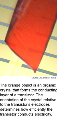
Researchers from Lucent Technologies' Bell Laboratories, Rutgers University and the University of Illinois have found that the orientation of crystalline organic semiconductors plays a big role in organic transistor performance. The researchers have developed a simple lamination manufacturing process for making transistors from the fragile organic material, and the resulting transistors have set a record for carrier mobility in organic transistors.
The researchers' method could lead to mass production techniques for organic transistors and light-emitting diodes.
The researchers' field-effect transistor is formed from organic rubrene crystal and titanium and gold electrodes and has a carrier mobility of 15.4 square centimeters per volt second, compared to typical organic semiconductor carrier mobilities of less than one square centimeter per volt second, according to John Rogers, a professor of materials science and engineering at the University of Illinois.
The silicon transistors commonly used in today's computer chips have carrier mobilities of 1,500 square centimeters per volt second, and other inorganic crystalline semiconductors can have carrier mobilities an order of magnitude higher than silicon.
The orientation of the molecules within the organic crystal and the spacing between the molecules contribute to the prototype's relatively high carrier mobility, said Rogers. Crystal molecules in the prototype transistor are spaced 1.44 nanometers apart in one direction and 0.72 nanometers in the perpendicular direction. Carrier mobility dropped to 4.4 square centimeters per volt second when the wide spacing of the crystal was aligned with the electrodes. A nanometer is one millionth of a millimeter.
The rubrene molecule has groups of atoms attached to its sides, and electrons flow along these side groups and along the backbone of the molecule. In the high-mobility orientation, the molecules' side groups are aligned, facilitating electron flow from molecule to molecule. "The orientation of the molecules relative to the electrodes of the transistors has a profound impact on the way [the] devices behave," said Rogers.
To test the relationship between orientation and performance in the organic crystal, the researchers developed a method of making field effect transistors that allowed them to repeatedly place, remove, rotate and replace the relatively fragile crystal on the transistor's electrodes. "We build all components of the transistor -- source/drain electrodes, gate dielectric, and gate electrode -- out of soft, conformable materials built on a soft, elastomeric substrate," said Rogers. "We then, at room temperature and without applied pressure, gently place the organic crystal, which is grown in a separate process... on the surface of this transistor stamp."
To make the transistors, the researchers placed a titanium-gold gate electrode on a silicone rubber surface, covered it with a thin film of silicone rubber and placed titanium-gold source and drain electrodes on top. They then simply placed the organic crystal over the electrodes and gently pressed one edge of the crystal. This caused the crystal to adhere to the silicone and metal due to the van der Waals force, which is the electrostatic attraction between atoms and molecules. "The soft contact forms very high-performance transistors in a way that avoids all of the hazards that conventional semiconductor processing poses to the organics," said Rogers.
The lamination method could be used in practical applications in three to five years, said Rogers.
Rogers' research colleagues were Bell Laboratories researchers Vikram Sundar, now at IBM, Jana Zaumseil, now at the University of Cambridge, Robert Willett, and Takao Someya, now at the University of Tokyo; Vitaly Podzorov and Michael Gershenson of Rutgers University; and Etienne Menard of the University of Illinois.
They published the research in the March 12, 2004 issue of Science. The research was funded by the National Science Foundation (NSF) and the U.S. Department of Energy.
Timeline: 3-5 years
Funding: Government
TRN Categories: Integrated Circuits; Materials Science and Engineering
Story Type: News
Related Elements: Technical paper, "Elastomeric Transistor Stamps: Reversible Probing of Charge Transport in Organic Crystals," Science, March 12, 2004
Advertisements:
April 7/14, 2004
Page One
Net plan builds in search
Robot guided by its voice
Angle speeds plastic transistor
Sturdy quantum computing demoed
Briefs:
DNA folds into paired pyramids
Fiber spun from nanotube smoke
Material boosts thermoelectricity
Nano ribbons coil into rings
Simulation maps nano patterns
Chip-camera combo tracks viruses

News:
Research News Roundup
Research Watch blog
Features:
View from the High Ground Q&A
How It Works
RSS Feeds:
News
Ad links:
Buy an ad link
| Advertisements:
|
 |
Ad links: Clear History
Buy an ad link
|
TRN
Newswire and Headline Feeds for Web sites
|
© Copyright Technology Research News, LLC 2000-2006. All rights reserved.