Process
promises better LCD production
By
Chhavi Sachdev ,
Technology Research NewsThe liquid crystal displays in your laptop screen and your cell phone were probably made using a process called rubbing that is almost a century old. The reason rubbing has prevailed is not because it is the best method -- indeed, there are many drawbacks to implementing it -- but because there has never been a viable substitute that could be used for large-scale manufacturing.
Researchers at IBM have endeavored to address the display industrys complaints by developing a cheaper, easier, higher-yield non-contact technique for aligning the liquid crystals.
In the process of rubbing, a giant roller wrapped in velvet is rubbed on a polymer surface that has been baked in a furnace. Liquid crystal molecules on the surface align themselves in the direction of the motion. The new process, in contrast, does not make any contact with the surface. Atoms shot from an ion gun to the surface knock out all but those molecules that oriented in the same direction the ions are traveling, said Praveen Chaudhari, a scientist at IBM and the lead researcher of the project.
The biggest limitation of the rubbing technique is that it introduces debris. To keep fibers from the rubbing cloth out of other manufacturing processes, the rubbing machine must be placed in a separate clean-room environment.
The technique is also somewhat unreliable because the rollers can degrade unevenly, causing defects that may go undetected until hundreds of displays have been manufactured. Rubbing can leave streaks which degrade image quality and can produce an electrostatic discharge that affects the circuitry of the display. Replacing the rubbing cloth also delays production.
The idea behind the non-contact alignment method is simple, according to Chaudhari. An ion beam is fired at diamond-like carbon and the angle of the beam determines the alignment of the liquid crystal molecules. Atoms in diamond-like carbon are interconnected in a network that has no order. The random network has rings of atoms in it. A given ring can be described by a plane, explained Chaudhari. A perpendicular ion beam, therefore, "tends to have a higher probability of knocking [perpendicular] atoms out, than if the plane is parallel to [it]" he said.
"What you're left with after you keep shooting atoms are those planes that are parallel to the ion beam. All the ones that are perpendicular are destroyed. It's like a Darwinian process of selection. The liquid crystals align themselves along [the surviving planes] and you're done," said Chaudhari.
The researchers replaced the baked polymer surface with a layer of diamond-like carbon film vapor-deposited on a substrate. Diamond-like carbon is widely used in the electronics industry, and therefore readily available. The low energy ion gun that replaced the rubbing roller is also commercially available. "So the tools and manufacturing experience already existed," said Chaudhari.
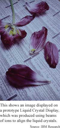
The result is a debris-free, reliable, cost-effective, highly scalable, and more environmentally friendly method than the one currently in use, according to Chaudhari. IBM used the process to make a prototype LCD, "Bertha," that measures 22 inches and has 3,840 by 2,400 pixels.
"The technique is certainly novel," said Satyendra Kumar, a professor of physics and chemical physics at Kent State University. "Although they have demonstrated in their laboratory it works very well, I have my reservations about its implementation on an assembly line. Basically, each plate will have to be put in a vacuum and bombarded by ions. This hardly appears more convenient or low cost than rubbing," he said. "Other techniques, such as UV exposure, appear far more attractive and practical," he added.
No other rubbing technique has been used to demonstrate a large display area, but the IBM researchers "have already demonstrated a working large area LCD using this technique," said N. V. Madhusudana, a professor at the Raman Research Institute in Bangalore, India. He also pointed out, however, that the IBM technique would require additional vacuum lines to process the displays.
IBM has established a pilot assembly line, Chaudhari said. The researchers expect large-scale production of the LCD's by the end of 2001.
The research was published in the May 3, 2001 issue of the journal Nature and prototypes of the display were shown at the Society of Information Display meeting in June, 2001. The research was funded by IBM.
Chaudhari's colleagues were James Lacey, James Doyle, Eileen Galligan, Shui-Chi Alan Lien, Alesandro Callegari, Gareth Hougham, Norton D. Lang, Paul S. Andry, Richard John, Kei-Hsuing Yang, Minhua Lu, Chen Cai, James Speidell, Sampath Purushothaman, John Ritsko, Mahesh Samant, Joachim Stöhr, Yoshiki Nakagawa, Yoshimine Katoh, Yukito Saitoh, Kazumi Sakai, Hiroyuki Satoh, Shuichi Odahara, Hiroki Nakano, Johji Nakagaki & Yasuhiko Shiota at IBM research.
Timeline: now
Funding: corporate
TRN Categories: Materials Science and Engineering
Story Type: News
Related Elements: Technical paper, "Atomic-beam alignment of inorganic materials for liquid-crystal displays," Nature, May 3, 2001.
Advertisements:
June 13/20, 2001
Page One
Stressed silicon goes faster
Artificial synapses copy brain dynamics
DNA device detects light signals
Lightwaves channel atoms to make chips
Process promises better LCD production
News:
Research News Roundup
Research Watch blog
Features:
View from the High Ground Q&A
How It Works
RSS Feeds:
News
Ad links:
Buy an ad link
| Advertisements:
|
 |
Ad links: Clear History
Buy an ad link
|
TRN
Newswire and Headline Feeds for Web sites
|
© Copyright Technology Research News, LLC 2000-2006. All rights reserved.