Lightwaves
channel atoms to make chips
By
Eric Smalley,
Technology Research NewsA common method for adding a very thin layer of material to a surface is to condense a vapor of the material, often a metal, and let its atoms rain down.
An important process in chipmaking is to use one substance to dope, or chemically alter, a layer of another in order to change its electrical or optical properties in certain areas. For example, the wires on a computer chip are made by doping the silicon in lines to make those areas conduct electricity.
Researchers at the University of Konstanz in Germany have come up with a technique that allows them to condense two or more substances at once and to direct the "rainfall" of one of them to specific places on the surface, effectively doping the layer as it's made.
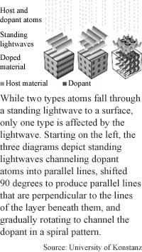
The key is using standing lightwaves as a set of lenses to focus the atoms of one of the substances as they fall to the surface. Standing lightwaves are lightwaves that are reflected back on themselves so that the waves' crests and troughs remain stationary in space.
Other researchers have used lightwave lenses to focus beams of atoms. The University of Konstanz researchers have gone a step further by tuning the frequency of the standing lightwaves to match the resonance frequency of one of the substances. The frequency-matched substance is focused by the lightwave lenses while the other substance is mostly unaffected.
"The... force is strongly enhanced when the laser wavelength is extremely close to the resonance frequency of the deposited material," said Dirk Jürgens, a graduate student at the University of Konstanz. "Therefore another material... will interact only very weakly with the light field and the atomic trajectories are not altered."
This allows the researchers to deposit one of the substances in patterns and the other in a homogeneous layer all at once.
The researchers have used the method to deposit chromium and magnesium fluoride onto a surface at the same time. "The dopant material -- in our case chromium -- [is] focused during deposition, whereas the host material is deposited homogenously," said Jürgens.
Doping magnesium fluoride with chromium increases its refractive index, or the angle at which magnesium fluoride bends light. By alternating areas of doped and pure magnesium fluoride, thereby alternating the refractive index, the researchers made a photonic bandgap layer that blocked a specific frequency of light. Photonic bandgap materials are used in optical communications devices to channel light.
The method allowed the researchers to easily discover that chromium was not a useful dopant for magnesium fluoride because the refractive index change was not enough to produce a practical photonic bandgap material, according to the researchers.
The researchers were also able to use the technique to dope materials in three-dimensional patterns by changing the position of the lightwave lenses for successive layers.
This method of changing optical properties using optical-deposition interactions is "quite remarkable," said Sandip Tiwari, a professor of electrical and computer engineering at Cornell University and director of the Cornell Nanofabrication Facility. "It does provide a convenient means to [form] three-dimensional structures with optical bandgaps. At small dimensions, this will be an intriguing and, if applicable, convenient technique that does not rely on complicated lithography and [the] reproduceability issues associated with it," he said.
The technique could be used for research purposes in the next two to five years, said Markus K. Oberthaler, head of atom optics research at the Konstanz Optics Center. "After that, [it] will be used for very specific applications. It is very unlikely that the method will enter big production lines. If so, that will be [at the] earliest in 10 to 15 years," he said.
Jürgens' and Oberthaler's research colleagues were Thomas Schulze, Tobias Müther, Björn Brezger, Tilman Pfau and Jürgen Mlynek of the University of Konstanz. They published the research in the March 19, 2001 issue of the journal Applied Physics Letters. The research was funded by the University of Konstanz, the Konstanz Optics Center and the European Union.
Timeline: 2-5 years; 10-15 years
Funding: University; Government
TRN Categories: Semiconductors; Materials Science and Engineering
Story Type: News
Related Elements: Technical paper, "Structure doping with light forces," Applied Physics Letters, March 19, 2001
Advertisements:
June 13/20, 2001
Page One
Stressed silicon goes faster
Artificial synapses copy brain dynamics
DNA device detects light signals
Lightwaves channel atoms to make chips
Process promises better LCD production
News:
Research News Roundup
Research Watch blog
Features:
View from the High Ground Q&A
How It Works
RSS Feeds:
News
Ad links:
Buy an ad link
| Advertisements:
|
 |
Ad links: Clear History
Buy an ad link
|
TRN
Newswire and Headline Feeds for Web sites
|
© Copyright Technology Research News, LLC 2000-2006. All rights reserved.