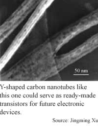
Forked nanotubes are tiny transistors
By Eric Smalley, Technology Research NewsThe idea of making computer chips based on carbon nanotubes gained further credibility this month with research showing that Y-shaped nanotubes could be ready-made transistors.
The research showed that the forked nanotubes amplify current, a necessary property for transistors. The nanotubes also allow current to flow in only one direction, meaning they could be used to convert alternating current to direct current.
Nanotube-based circuits have the potential to be much smaller than today's semiconductor technology. The smallest features possible with today's photolithography are about 125 nanometers wide. The forked nanotubes are as small as 15 nanometers in diameter. Smaller circuits means more can fit on a computer chip, yielding more powerful computers.
Transistors, which are the basic building blocks of virtually all modern electronics including computers, have three terminals, or points of contact. The forked nanotubes naturally have three terminals. However, the researchers have only tested the forked nanotubes using two points of contact.
"[It's] hard to make reliable contact to each of the three terminals," said Jingming Xu, an engineering and physics professor at Brown University and the principal investigator.
Still, using two points of contact was enough to demonstrate the electronal properties of the forked nanotubes, he said.
"The fact that the Y-junction nanotubes [allow current flow in one direction] says it is already a functional device -- a diode of molecular scale. The fact that the Y-junction [nanotube] is a three-terminal structure [that amplifies current] says it should function like a transistor of molecular scale," Xu said.
The key to making the forked nanotubes act as transistors lies in making the two branches narrower than the stem, which gives the branches and stem different electrical properties.
"In general, electronic devices based on nanotubes hold great promise for the future," said Jianping Lu, an associate professor of physics and materials science at the University of North Carolina. "Perhaps it's the only material we know of which could potentially replace silicon technology."
The Y-junction nanotube research is one example of several projects that experimentally demonstrate nanotubes serving as electronic devices, said Lu. However, the forked nanotubes are larger, multi-wall nanotubes, and most researchers are looking to use smaller, single-wall nanotubes for electronics, he said.
"This is one step on the road. Perhaps if you can grow something on the larger scale... it's not completely out of the question that you can grow [Y-junctions] out of single-wall nanotubes or down to the one nanometer scale," Lu said.
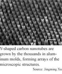
The researchers fabricated the forked nanotubes by injecting a chemical vapor at high temperature into aluminum molds containing a powder catalyst. The vapor condensed on the sides of the molds, forming the hollow nanotubes. The researchers then chemically removed the aluminum, leaving the nanotubes. They can be made with stem diameters ranging from 15 to 100 nanometers.
"The significance [of Xu's work] is actually showing you can grow three-terminal devices en masse," said Lu.
Xu declined to say when or even if nanotubes could be used to make integrated circuits.
"No one knows what the future computing architecture will be, thus no [one knows] what [components] should be used, "he said.
Xus colleagues were Chris Papadopoulos, Andrei Rakitin and Jing Li of the University of Toronto, and Alex S. Vedeneev of the Russian Academy of Sciences. The researchers published their work in the October 16, 2000 issue of the journal Physical Review Letters. The research was funded by the Office of Naval Research.
Researchers at the Jawaharlal Nehru Centre for Advanced Scientific Research in Bangalore, India reported a similar technique for fabricating Y-shaped carbon nanotubes in the October 16, 2000 issue of the journal Applied Physics Letters.
Timeline: Unknown
Funding: Government
TRN Categories: Nanotechnology; Integrated Circuits; Semiconductors and Materials
Story Type: News
Related Elements: Photo 1, Photo 2; Technical paper "Electronic Transport in Y-Junction Carbon Nanotubes" in Physical Review Letters, October 16, 2000, Technical paper "Nanoelectronics: Growing Y-junction carbon nanotubes" in Nature, November 18, 1999
Advertisements:
October 25/November 1, 2000
Page One
Disk-on-a-chip takes shape
Shaky table top sorts parts
Forked nanotubes are tiny transistors
Society goes on data binge
Pulse harbors magnetic mystery
News:
Research News Roundup
Research Watch blog
Features:
View from the High Ground Q&A
How It Works
RSS Feeds:
News
Ad links:
Buy an ad link
| Advertisements:
|
 |
Ad links: Clear History
Buy an ad link
|
TRN
Newswire and Headline Feeds for Web sites
|
© Copyright Technology Research News, LLC 2000-2006. All rights reserved.